

Theoretical evaluation of contact stack for high efficiency c-Si IBC heterojunction solar cells
In the 8th work package of NextBase project, TUDelft has recently made available for NextBase partners a scientifically-accurate and numerically-stable TCAD Sentaurus-based opto-electrical modelling platform. This platform (i) captures in great detail the physics of carrier-selective passivating contacts, (ii) unveils transport loss mechanisms across emitter and back surface field stacks in c-Si heterojunction solar cells and (iii) evidences the criticality of a well-designed emitter stack (i.e. the p-type finger of the NextBase IBC solar cell) [1][2].
It has been found that, as long as the activation energy value of the p-type doped layer remains below 200 meV, any transparent conductive oxide (TCO) can be used. Alternatively, if the activation energy value of the p-type layer oscillates between 200 and 400 meV, a more careful choice of the TCO has to be made (TCO work function above 5 eV) in combination with a i/p stack thickness beyond 15 nm. Ultimately, wide bandgap p-type SiOx or SiCx could be deployed to also enhance band banding, leading to high-quality surface passivation and carriers transport.
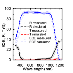
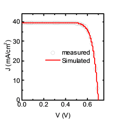
After calibrating the platform with specific partner’s IBC heterojunction solar cells, from the interaction of geometrical dimensions (fingers’ pitch, emitter-to-pitch ratio, layers thickness, etc.) with materials’ properties (bandgap, activation energy, work function, trap states distribution, etc.), it is possible to indicate optimization strategies to achieve high efficiency for each specific case. TUDelft modelling platform has been already successfully calibrated to three c-Si IBC devices (TUDelft [1], IMEC and CSEM), that are very different in terms of overall design and deployed materials. Each time, with one set of parameters, the optical and electrical behaviour of these three IBC solar cells could be perfectly matched to measurements. In the figure below (left, centre), the case of a c-Si IBC solar cell based on doped poly-Si carrier-selective passivating contacts fabricated at TUDelft is reported. Simulation efforts by TUDelft are currently ongoing to provide each partner in NextBase project capable of making complete devices with solar cell design guidelines enabling efficiency beyond 26%.
 |
 |
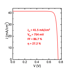 |
| (Left) Simulated and measured wavelength-dependent external quantum efficiency (EQE), reflectance (R) and transmittance (T) spectra and (centre) simulated and measured current density – voltage characteristic of a c-Si IBC solar cell based on doped poly-Si carrier-selective passivating contacts fabricated at TUDelft. (Right) Record c-Si IBC heterojunction solar cell simulated with TUDelft modelling platform and based on technology currently available in NextBase consortium. | ||
At the past 33rd EU PVSEC (2017) [1] and SiliconPV (2018) [2], Dr. Paul Procel from TUDelft has also reported on the ultimate conversion efficiency achievable by c-Si IBC heterojunction solar cells with technology currently available in NextBase consortium (η > 27%, see figure above on the right-hand side). For this work, he has been given the SiliconPV Award, which is granted to the 10 best-ranked contributions of SiliconPV 2018 and selected among more than 200 blind-reviewed submissions. Further developments of TUDelft modelling work within the NextBase project will be reported at the 7th World Conference on Photovoltaic Energy Conversion [3].
[1] P. Procel, G. Yang, O. Isabella, M. Zeman, Opto-electrical modelling of IBC solar cells based on poly-Si or heterojunction carrier-selective passivating contacts, 33rd European PV Solar Energy Conference and Exhibition, Amsterdam, the Netherlands (2017).
[2] P. Procel, G. Yang, O. Isabella, M. Zeman, Theoretical evaluation of contact stack for high efficiency IBC-SHJ solar cells, SiliconPV, Lausanne, Switzerland (2018).
[3] P. Procel, G. Yang, O. Isabella, M. Zeman, Understanding transport mechanisms of high efficiency IBC c-Si solar cells based on poly-Si or HTJ carrier-selective passivating contacts, 7th World Conference on Photovoltaic Energy Conversion, Waikoloa, Hawaii, U.S.A. (2018).