
Simulation studies of the optical and electrical losses of interdigitated rear-contact silicon heterojunction (IBC-SHJ) solar cells
In order to investigate the ultimate efficiency potential of interdigitated rear-contact silicon heterojunction (IBC-SHJ) solar cells, we have carried out detailed simulation studies of the optical and electrical losses in these devices. A realistic set of parameters was defined for the different layers and interfaces in the device, based on measurements on our actual layers and devices. Then, 2D-simulation studies of the electrical and optical properties of the cells were carried out using numerical device simulators.
Interestingly, some quite general conclusions could be drawn from the simulations:
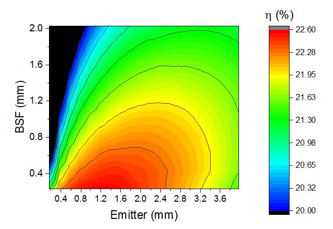
- As long as the passivation properties of different films (emitter / back surface field (BSF)) are at the same level, the ratio of emitter-vs-BSF coverage, and the absolute size of the contacts as defined by this ratio and the unit cell pitch, have a negligible influence on the open circuit voltage. The fill factor, on the other hand, is very sensitive to the contact size.
- For the simulated (realistic) materials properties, the optimum for the technological pitch is of the order of 0.5-1.5 mm. This is an important result, since it shows that highly efficient IBCs can be fabricated with industry-compatible low cost structuring techniques such as laser ablation, shadow masks or inkjet printing.
- Both emitter and BSF should be covered as thoroughly as possible by metal contacts. For example, metallization gaps of 50 µm lead to a slight decrease in solar cell fill factor (a few tenths of a percent abs.). Such a small gap width is technologically challenging, but feasible with today’s structuring techniques.
- Regarding optical properties, it could be demonstrated that the front side antireflection/light trapping structures currently available within NextBase are on par with those of the current world record IBC-SHJ cell, which account for ~1 mA/cm² photocurrent loss as compared to the maximally available 43.2 mA/cm² from c-Si wafers, or ~2.3%rel.
Currently, data is collected that will allow to calibrate the model to the different partners’ IBC structures. This “simulation toolbox” will then make it possible to distinguish between distinct contributions both on the optical as well as on the electrical losses, and to make quantitative assessments and optimizations more specifically for the different structures.