

Preliminary results Jülich
Highly transparent and conductive n-type microcrystalline silicon carbide (µc-SiC:H(n)) was investigated to be used as a window layer in combination with an ultra-thin tunnel oxide (SiO2) passivation layer for silicon heterojunction (SHJ) and interdigitated back conatacted (IBC) SHJ solar cells. Both µc-SiC:H(n) and SiO2 offer a large bandgap of 2.6-3.0 eV and > 8 eV, respectively, and provided a high implied open circuit voltage of up to 711 mV using textured silicon wafer. In addition, it is worth to highlight that no high temperature annealing or forming gas annealing step were needed and that the tunnel oxide was grown wet chemically at room temperature. These advantageous properties make µc-SiC:H(n)/SiO2 an attractive alternative to the classical front side designs of silicon homojunction or heterojunction solar cells. We found out that the implementation of µc-SiC:H(n) could improve the short circuit density for a two-side contacted design to 41 mA/cm² and for interdigitated back contacted design potentially to 43 mA/cm².
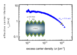
Fig. 1. Effective carrier lifetime as a function of excess carrier density Δn of a textured wafer passivated by an ultra-thin (~ 1.2 nm) SiO2 grown from HNO3 solution in combination with a 30 nm thick µc-SiC:H(n) layer grown by HWCVD.
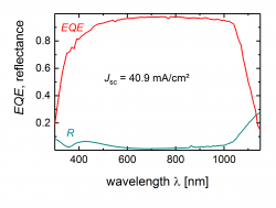
Fig. 2. External quantum efficiency and reflection of the SHJ solar cell with highest short circuit current density (Jsc). For FSF and emitter, µc-SiC:H(n)/SiO2 FSF and 10 nm i-a-Si:H/70 nm µc-SiO2:H(p) stacks were used, respectively.