

High-efficiency IBC-SHJ devices processing
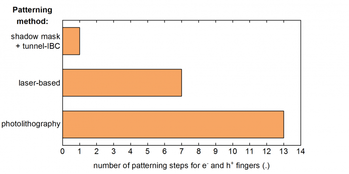
In WP5, several approaches for the processing of IBC-SHJ devices are compared, namely laser-based patterning techniques, photolithography and shadow mask patterning. Figure below shows the number of patterning steps required with each technique to pattern the electron and the hole collecting fingers in an IBC-SHJ device. Remarkably, the combination of shadow mask patterning with a tunnelling electron contact allows a very lean process flow, as only one single patterning step is required. This is a major leap towards a cost-effective process flow of IBC-SHJ devices.
Importantly, this process simplification is not done at the expenses of the device performances, as a champion IBC-SHJ solar cell with a certified efficiency of 25% was obtained with this approach.