

Characterized and numerical simulations (WP8)
Objective
WP8 aimed at developing specific characterization tools and simulations to support the development of the interdigitated back contacted (IBC) silicon heterojunction (SHJ) solar cells. WP8 supported in particular the development of electrode stacks and patterning design.
Results
The limiting factors of high efficiency IBC SHJ were clearly identified, thus accelerating the development of material with properties for high efficiency devices. The strategic support of accurate numerical simulations demonstrated an accelerated learning curve for the research and development of high efficiency IBC devices. All the joint work was presented at EUPVSEC 2019 explaining the compulsory material conditions and physical mechanisms for high-performant devices.
WP8 was really complex, involving people from 8 project partners. Instead of trying to overview all of it, let us focus on one of the results obtained in this work package and its latest practical development. The optimization of the IBC SHJ required measurement of the thickness of amorphous stripes with precision of roughly 1 nm, which was achieved by Raman based optical profilometry. This was identified as one of the project’s Key Exploitable Results, but we realized that it is too slow to be useful at the production lines. Thus we looked for adaptation of the technique which would allow imaging the stripes over all solar cell within seconds.
This target was successfully achieved by large area photoluminescence (PL) imaging using two different excitation wavelengths. The method is illustrated by figure 1.
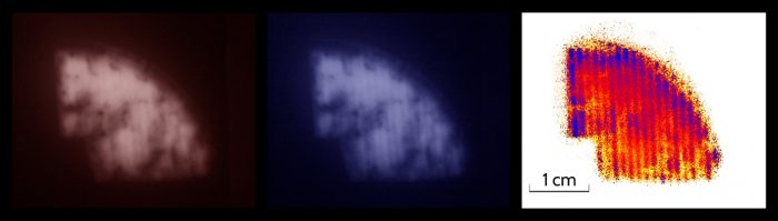
Figure 1: From left to right the PL image under the red illumination, PL image under the blue illumination and final image of amorphous stripes.
When the PL is excited by blue light, its intensity is lowered by absorption of the excitation light in the overlying amorphous silicon stripe. On the other hand, the stripes are very well transparent for the red light. Therefore, by comparing the blue and red images we can visualize the amorphous stripes, as shown in the right image.
Impact
Imaging of such extremely thin amorphous silicon structures on the silicon surface by Raman mapping was introduced in the very beginning of this project. This technique is very precise but also highly time-consuming. The PL imaging opens a way for fast everyday routine characterization procedure, which may be used even as an in-line characterization tool in production of IBC hetero-junction solar cells.
Lessons learnt
The very important lesson for us, as a research institute, was the interaction with companies and understanding what the needs for successful practical implementation of this new cell technology are.