
Novel layer stacks and contacting materials
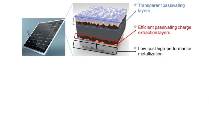
The main goals in the area of novel layer stacks and contacting materials are summarised in the figure below. Although no electrical contact is placed on the front-side of the wafer, some layers still have to be deposited to ensure that light is coupled in the silicon wafer and is not reflected out. Additionally, defects at the surface of the wafer should be suppressed to ensure optimal use of the generated electrical charges. This requires finely tuned materials, stacks of amorphous silicon and silicon nitride show promising properties towards that goal.
Furthermore, the extraction of the positive and negative charges at the rear side requires layers that present low resistance and easy patterning processability. Amorphous and doped nanocrystalline silicon layer stacks are to that respect very well suited and the key parameters of their fabrication which can make them efficient were identified along this project.